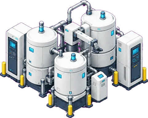
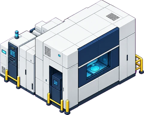
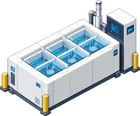
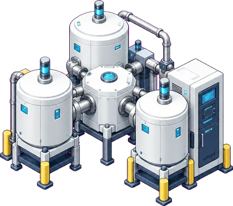
This is an abbreviated educational map, not a single standard path for actual fabrication. Sequences, repetitions, and materials differ between memory and logic, products, and process generations. Oxidation, ion implantation, heat treatment, planarization, interconnect formation, and other operations are not all shown as separate nodes. Companies illustrate roles based on public products and technologies; they are not lists of exclusive suppliers or verified counterparties. Economic significance and watch points are principle-based educational interpretations, not forecasts of earnings or share prices or investment recommendations.
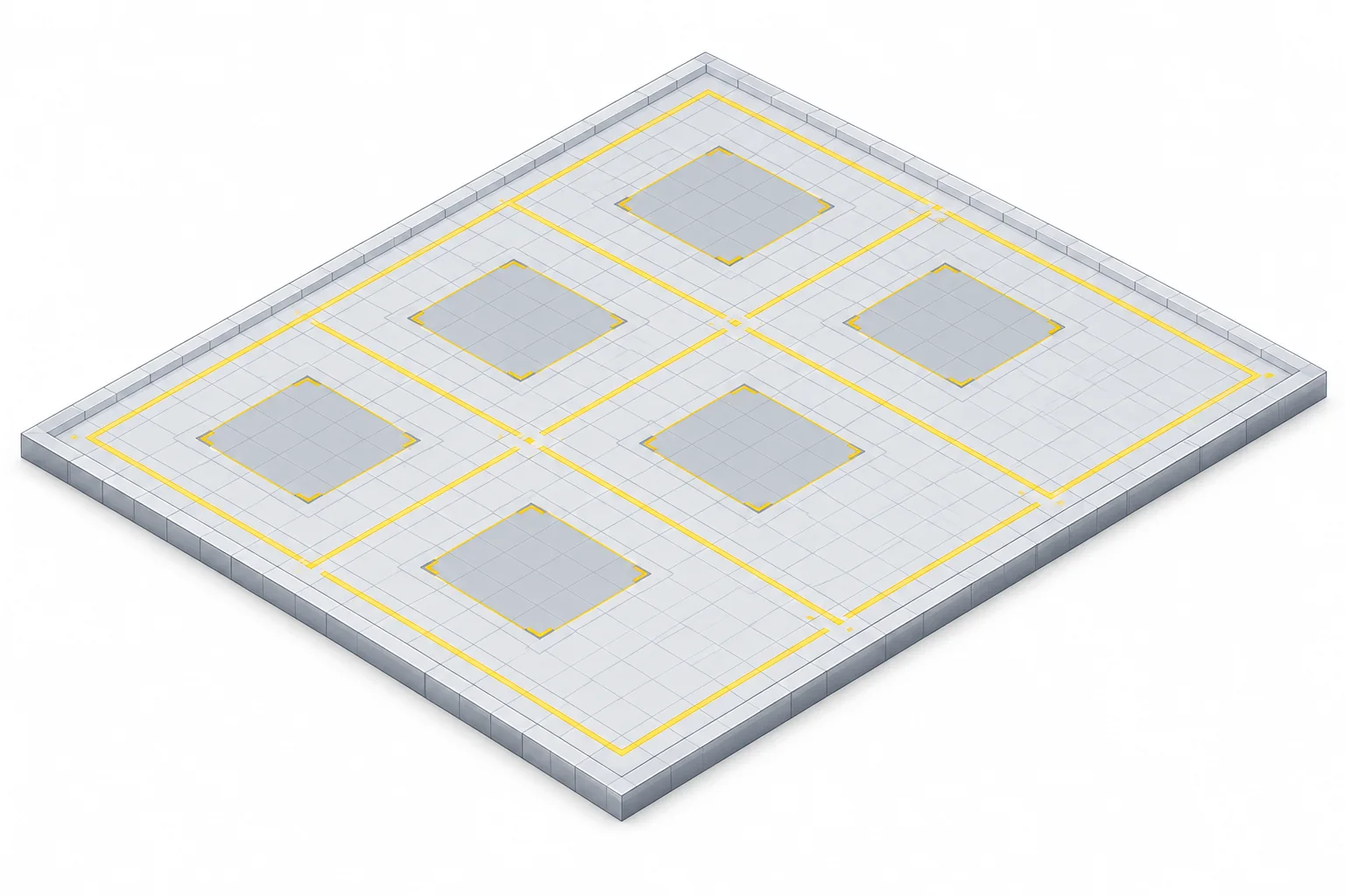
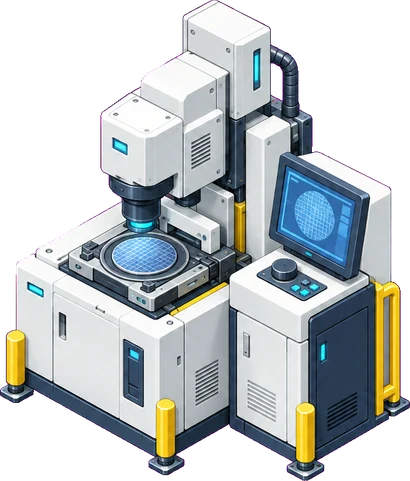
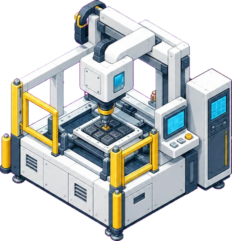
Educational diagram. Actual factory layouts and equipment proportions differ, and many processes repeat.
Materials
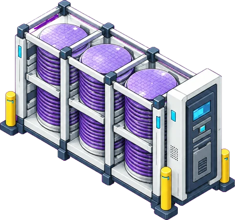
Wafers and substrates
Prepare the wafer material and surface on which circuits will be built.
Related companies
SUMCO
Silicon wafers, including polished and epitaxial wafers
Process explanation
A silicon wafer is a thin disc cut from a crystal and processed at the surface. Types such as polished and epitaxial wafers serve different purposes. Surface conditions and impurity control form the starting conditions for subsequent device fabrication.
Industry perspective
Why it matters
Examining input-wafer specifications and quality conditions, not only the number of finished chips, helps explain the link between materials and manufacturing.
Indicators to watch
What type of wafer does the product require?
What standards govern surface quality and impurities?