This is an abbreviated educational map, not a single standard path for actual fabrication. Sequences, repetitions, and materials differ between memory and logic, products, and process generations. Oxidation, ion implantation, heat treatment, planarization, interconnect formation, and other operations are not all shown as separate nodes. Companies illustrate roles based on public products and technologies; they are not lists of exclusive suppliers or verified counterparties. Economic significance and watch points are principle-based educational interpretations, not forecasts of earnings or share prices or investment recommendations.
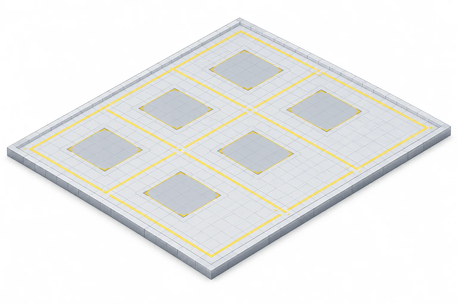
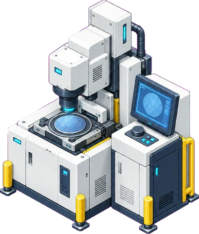
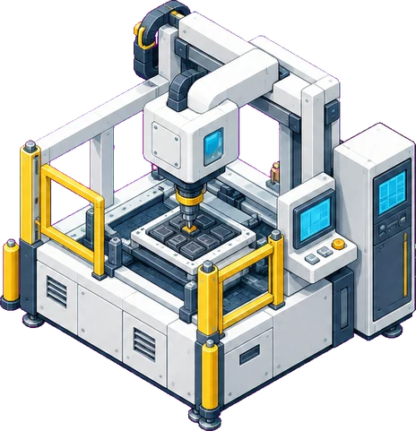
Educational diagram. Actual factory layouts and equipment proportions differ, and many processes repeat.
Back-end assembly
Electrical testing
Check that chips meet specified electrical characteristics and functions.
Related companies
Amkor Technology
Semiconductor packaging and wafer/package testing services
Advantest
Test systems checking semiconductor functions and electrical characteristics
Process explanation
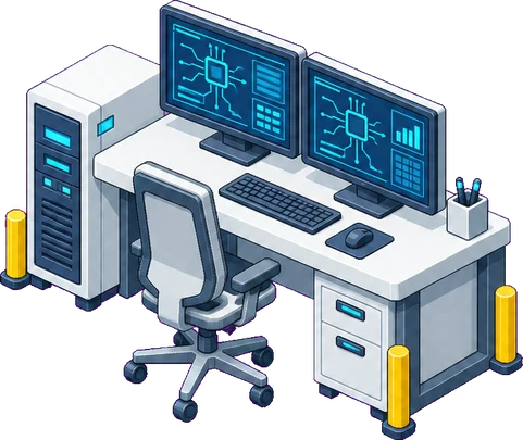
Test equipment supplies signals to semiconductors and measures responses to check operation. Testing occurs both at wafer stage and after package assembly. Test items and conditions are selected for the target chip and required quality.
Industry perspective
Why it matters
Examining defect-detection coverage alongside inspection time helps explain the relationship between quality assurance and production costs.
Indicators to watch
Is this testing at wafer or package stage?
Were test time and detection coverage compared together?