

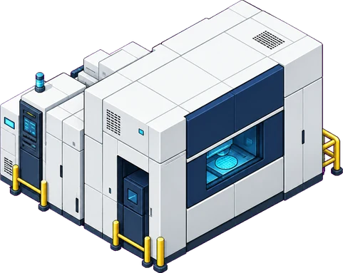
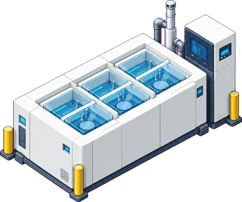
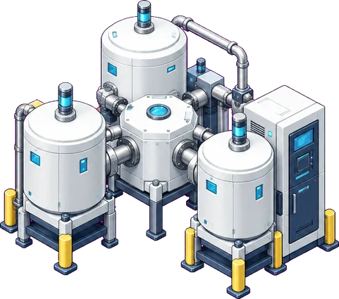
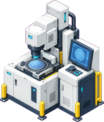
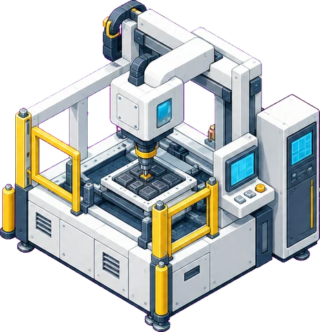
Back-end assembly
Packaging and connections
Protect chips and electrically connect them to external components or other chips.
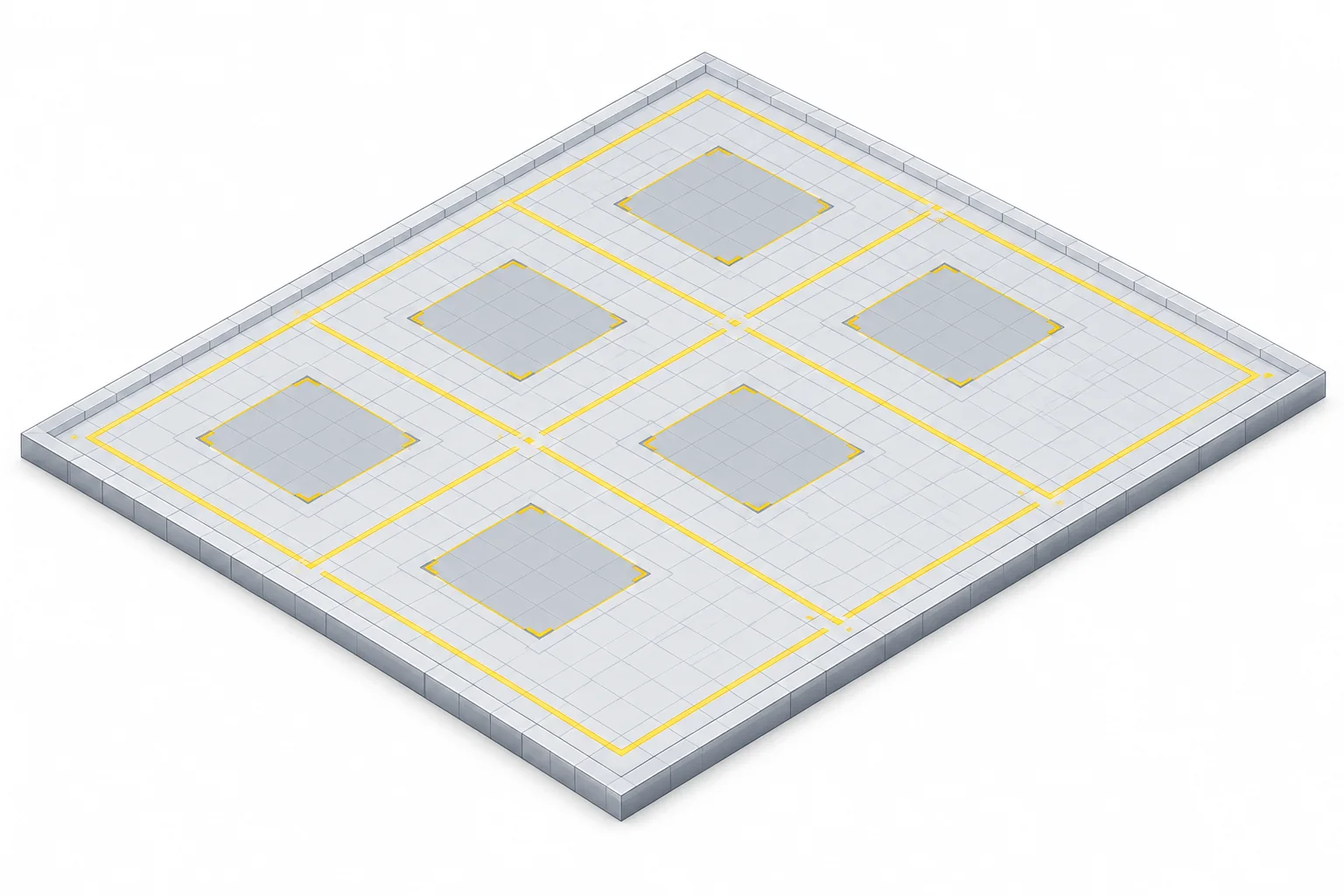
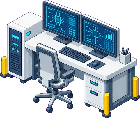
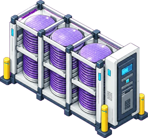
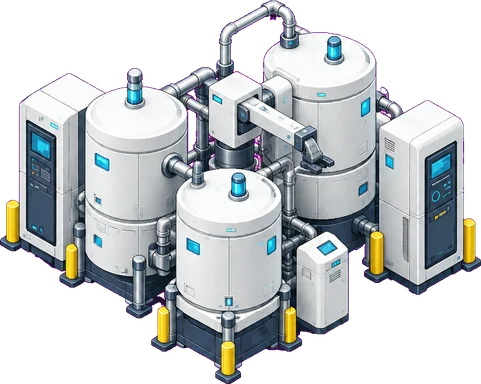
Concept diagram · not to scale
Related companies
Samsung Electronics
An example here of foundry manufacturing, design support, and packaging roles
Amkor Technology
Semiconductor packaging and wafer/package testing services
ASE
SiP and packaging technologies integrating multiple chips
SK hynix
DRAM memory, including HBM, and stacking technology
Process explanation
Packaging connects and protects dies so they can be used in systems. Approaches include SiP integrating multiple chips in a package, and 2.5D and 3D. Connections and thermal management both matter; not all packages have the same structure.
Industry perspective
Why it matters
Examining inter-chip connections and assembly conditions, not only individual-chip performance, helps explain the relationship between system performance and cost.
Indicators to watch
- How do connections and thermal management change when multiple chips are combined?
- Were assembly difficulty and the test plan considered together?
Sources
- Semiconductor Packaging Solutions ↗Amkor Technology · Checked 2026-10-09
- IC Semiconductor Test Services ↗Amkor Technology · Checked 2026-10-09
- Foundry Overview ↗Samsung Semiconductor · Checked 2026-10-09
- System in Package (SiP) ↗ASE · Checked 2026-10-09
- Continuing to Make HBM History: The Story of SK hynix’s HBM Development ↗SK hynix · Checked 2026-10-09
- Future Memory Technologies: Evolutionary Memory ↗SK hynix · Checked 2026-10-09