This is an abbreviated educational map, not a single standard path for actual fabrication. Sequences, repetitions, and materials differ between memory and logic, products, and process generations. Oxidation, ion implantation, heat treatment, planarization, interconnect formation, and other operations are not all shown as separate nodes. Companies illustrate roles based on public products and technologies; they are not lists of exclusive suppliers or verified counterparties. Economic significance and watch points are principle-based educational interpretations, not forecasts of earnings or share prices or investment recommendations.
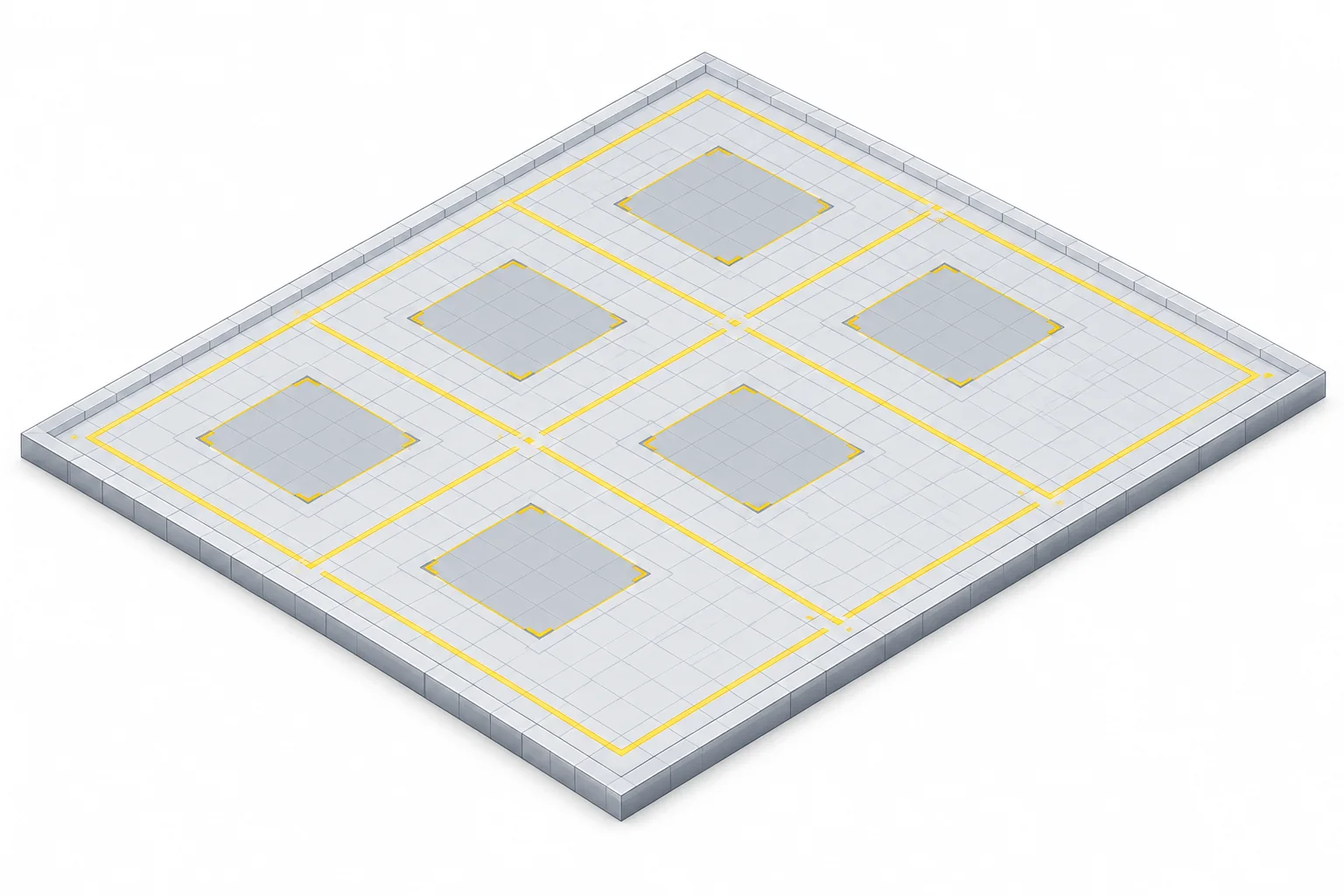
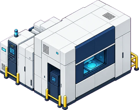
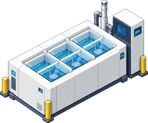
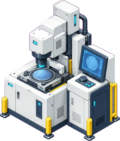
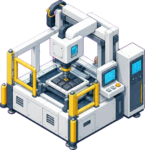
Educational diagram. Actual factory layouts and equipment proportions differ, and many processes repeat.
Design
Design and verification
Define the required functions as circuits and verify operation before manufacturing.
Related companies
Synopsys
EDA and semiconductor IP for circuit design and verification
Samsung Electronics
An example here of foundry manufacturing, design support, and packaging roles
Process explanation
Designers consider constraints such as performance, power, and area together. EDA is software supporting circuit design and verification; IP consists of reusable design assets. Manufacturing-process and package conditions must also be addressed during design.
Industry perspective
Why it matters
An economic reading can examine design productivity alongside the burden of rework when errors are found late.
Indicators to watch
Were performance improvements compared with power and area constraints?
Does verification cover software and manufacturing conditions?