This is an abbreviated educational map, not a single standard path for actual fabrication. Sequences, repetitions, and materials differ between memory and logic, products, and process generations. Oxidation, ion implantation, heat treatment, planarization, interconnect formation, and other operations are not all shown as separate nodes. Companies illustrate roles based on public products and technologies; they are not lists of exclusive suppliers or verified counterparties. Economic significance and watch points are principle-based educational interpretations, not forecasts of earnings or share prices or investment recommendations.
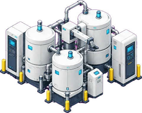
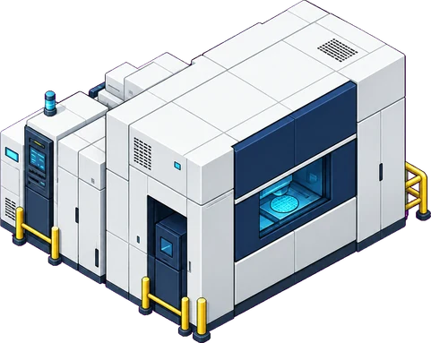
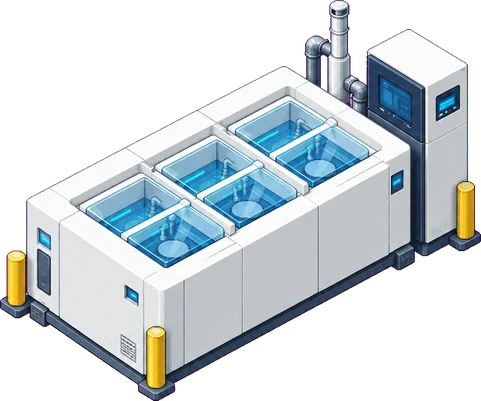
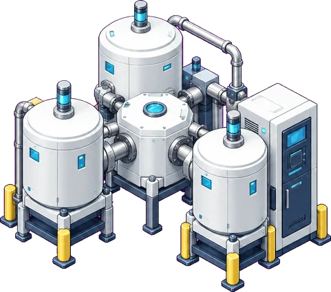
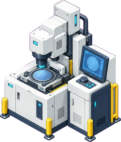
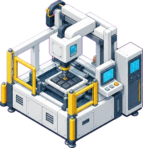
Educational diagram. Actual factory layouts and equipment proportions differ, and many processes repeat.
Demand
Applications and systems
Combine computation, memory, and connections to meet the requirements of real services and devices.
Related companies
NVIDIA
Data-center accelerated computing platforms
SK hynix
DRAM memory, including HBM, and stacking technology
Process explanation
Data-center accelerated computing uses memory and software as well as computing devices. HBM is a type of memory that stacks and connects multiple DRAM dies to provide high bandwidth. Application requirements in turn affect priorities in design, manufacturing, and packaging.
Industry perspective
Why it matters
Asking about computation, data movement, and power required for actual workloads—not just a particular chip’s specifications—is a starting point for understanding industry demand.
Indicators to watch
Is the workload constrained by computation, memory, or data movement?
Were component performance and actual system conditions distinguished?