This is an abbreviated educational map, not a single standard path for actual fabrication. Sequences, repetitions, and materials differ between memory and logic, products, and process generations. Oxidation, ion implantation, heat treatment, planarization, interconnect formation, and other operations are not all shown as separate nodes. Companies illustrate roles based on public products and technologies; they are not lists of exclusive suppliers or verified counterparties. Economic significance and watch points are principle-based educational interpretations, not forecasts of earnings or share prices or investment recommendations.
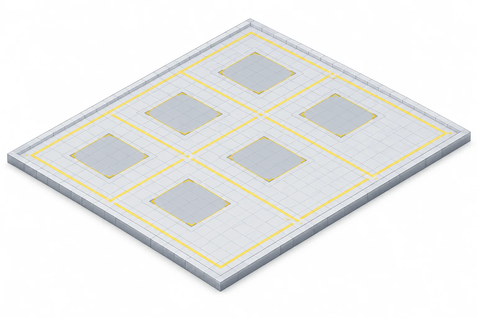
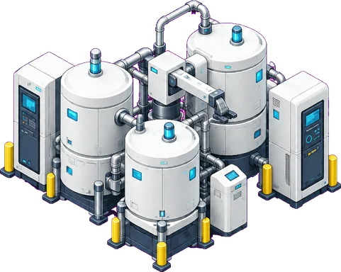
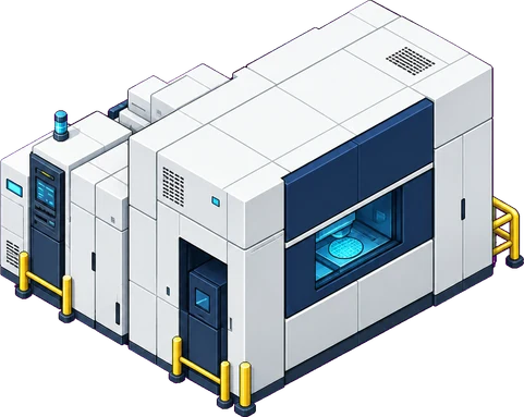
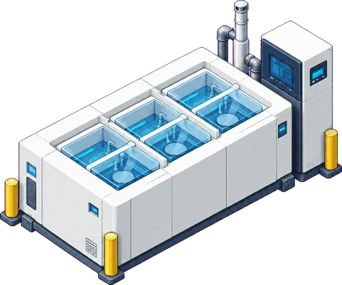
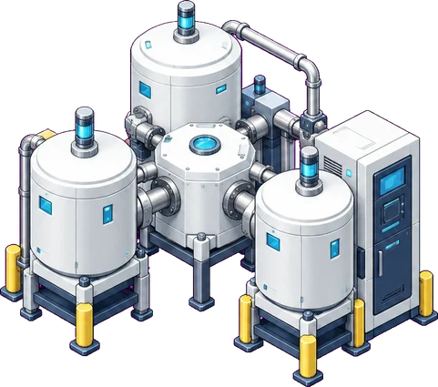
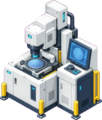
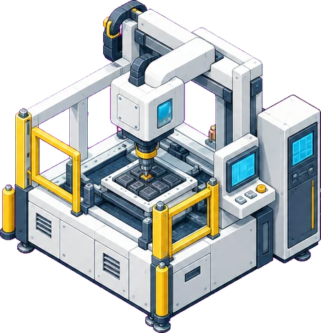
Educational diagram. Actual factory layouts and equipment proportions differ, and many processes repeat.
Process control
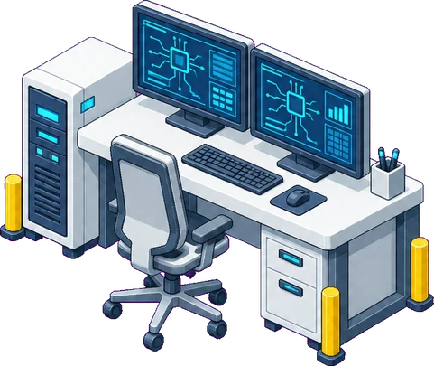
Metrology and inspection
Check dimensions and defects to provide evidence for adjusting manufacturing conditions.
Related companies
ASML
DUV and EUV lithography equipment, plus metrology and inspection solutions
KLA
Semiconductor metrology, inspection, and process-control solutions
Process explanation
Metrology measures film thickness and pattern dimensions, while inspection detects defects and contamination. Results help identify causes and adjust processes. These operations occur at multiple manufacturing points and differ from electrical testing of completed chips.
Industry perspective
Why it matters
This feedback checks whether processes work as designed. Considering measurement speed and detection capabilities together helps explain the cost of yield management.
Indicators to watch
Are defects to detect distinguished from dimensions to measure?
Do inspection results lead to actual process adjustments?