This is an abbreviated educational map, not a single standard path for actual fabrication. Sequences, repetitions, and materials differ between memory and logic, products, and process generations. Oxidation, ion implantation, heat treatment, planarization, interconnect formation, and other operations are not all shown as separate nodes. Companies illustrate roles based on public products and technologies; they are not lists of exclusive suppliers or verified counterparties. Economic significance and watch points are principle-based educational interpretations, not forecasts of earnings or share prices or investment recommendations.
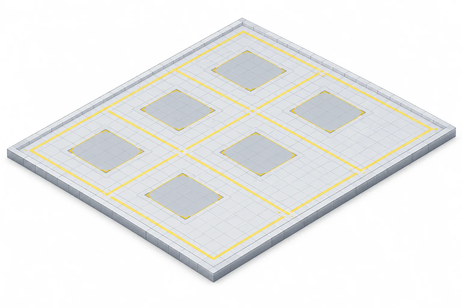
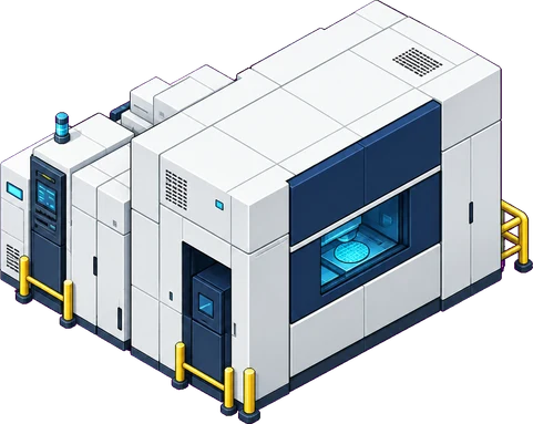
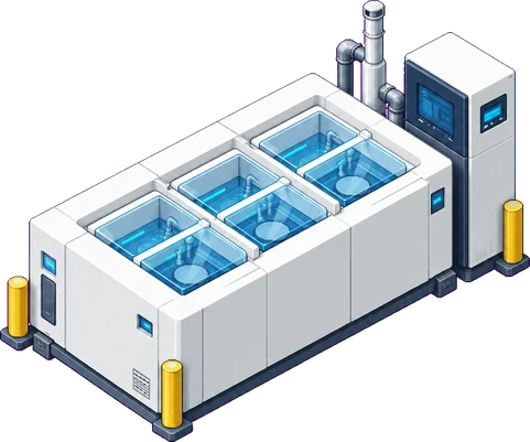
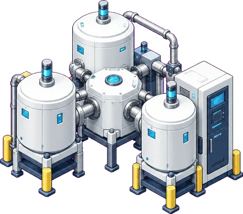
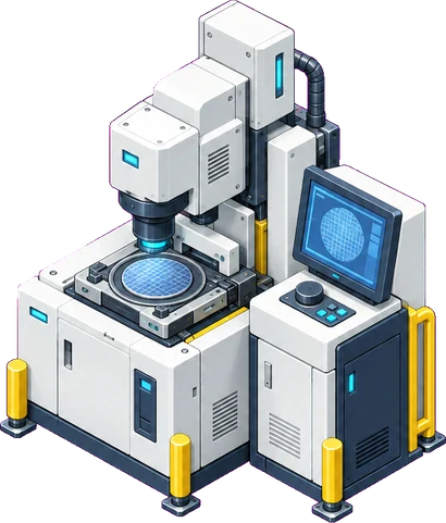
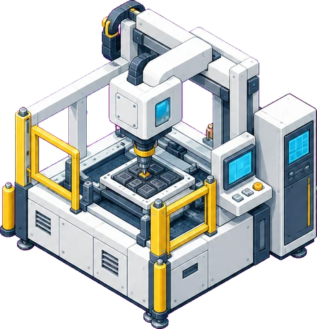
Educational diagram. Actual factory layouts and equipment proportions differ, and many processes repeat.
Front-end fabrication
Lithography
Use light to transfer circuit patterns to photoresist.
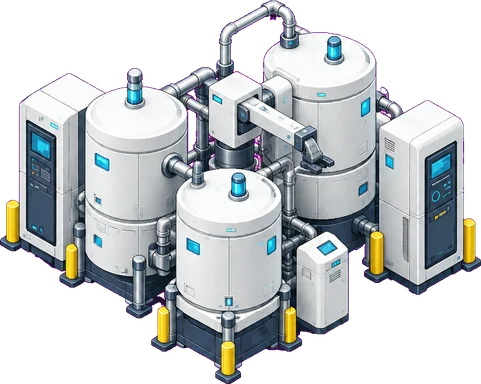
Concept diagram · not to scale
Related companies
ASML
DUV and EUV lithography equipment, plus metrology and inspection solutions
Tokyo Electron
Manufacturing equipment for deposition, coating/development, etching, and cleaning
Process explanation
Photoresist is applied to a wafer and lithography equipment transfers a pattern. Developing the light-sensitive resist leaves a pattern for the next process. Lithography methods such as DUV and EUV, and alignment accuracy between layers, are important.
Industry perspective
Why it matters
Considering small-pattern capability together with throughput helps explain trade-offs between precision and production costs.
Indicators to watch
What resolution and alignment accuracy does this layer need?
Are resist, development, and metrology conditions aligned as well as exposure?